
While testing this device, do not overload, do not load asymmetrically. For checking your system, remove nixie and load secondary winding of transformer with simple resistor.
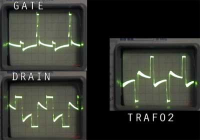
Download small (~500kb XVid AVI): with oscillograms. And now take a note, that on the “drain” oscillogram you see other phase pulses. Even when mosfet if in off stage, the induction from other primary winding cause voltage to appear. This may kill mosfet. And if load is unbalanced or not ideal, you can find lots of parasitic oscillations. So design engineer must take care of them. Parasitic oscillations can be killed with “snublers”- simple RC network on transformer windings. This devices takes some of the high frequency power and dissipates it.
And now lets look in internet:
Half-bridge and full-bridge |
Push-pull |
Forward converter |
|
minimum mosfet voltage rating |
supply voltage plus a safety margin
230VAC*1,414 + 50V |
double the supply voltage plus a large safety margin 2*230VAC*1,414+100V |
double the supply voltage plus a large safety margin 2*230VAC*1,414+100V |
other mosfet properties |
medium voltage 400V fets, so a <0.2 Ohm channel resistance is typical => high current, low loss |
high voltage 800V fets, >2.0 Ohm channel resistance is typical => low current, high loss |
high voltage 800V fets, >2.0 Ohm channel resistance is typical => low current, high loss |
mosfet body diode: |
must be disabled, otherwise mosfets explode if supply <50VDC: if supply >50VDC: |
can be ignored |
can be ignored |
realistic power levels |
many kW |
some 100W |
some 100W |
what limits the power level |
base-feed transformer core power handling capability (saturation, induced currents causing core heating) mosfet current ratings (paralleling more than two fets, the right way, mosfet switching and conduction losses |
primary leakage inductance, huge voltage spikes (up to kV range) at increasing power levels, makes use of snubber circuits imperative (=>high heating losses and low efficiency, and high circuit complexity) >=800V fets are expensive and can’t handle much current |
(same as for push-pull) |
transformer design |
needs only one primary transformer design non-critical |
needs two identical and well coupled primaries, critical design – requires skills! ;o) |
critical design, only one primary only the first quadrant of the ferrite cores’ B-H curve is used, i.e. |
base feed transformer volt-seconds (Vs) imbalance: |
full-bridge: minimal danger of saturation, Vs imbalance mainly due to slight differences in mosfet channel on-resistances half-bridge: if the primary has a series coupling capacitor, then Vs |
major problems with Vs imbalance as fully identical pri windings are almost impossible to make. The driver circuit absolutely must have pulse-by-pulse current limiting. |
|
tuneable down to DC / 0Hz |
yes, by using a primary series coupling capacitor |
no (short-circuit at 0 Hz) |
no (short-circuit at freq towards 0 Hz) |
problems |
grief with gate drive transformers or floating channel mosfet driver ICs or optocoupler-tweaking |
grief with mosfets constantly dying on overvoltage, gate drive noise |
(same as for push-pull) |
Pingback: Savel brain dump in English! » Blog Archive » TL494 - magic chip, Part 5
Pingback: Savel brain dump » Blog Archive » TL494 - universali mikroschema, 5 dalis
THANK YOU SO MUCH!!!!
YOUR TUTORIAL SAVED MY DAY.
Dear sir,
kindly provide me with a schematic and trafo construction details for a 18V 30A smps, input 180v… 260v.
Hello, thank you for your tutorial.
I wish I could adjust the output voltage pulse width feedback pin, but if the input voltage varies, the output voltage as well. Is there a way to solve this problem,
For “Padmanabhan”
There is a very good site for calculating transformer PWM here.
w w w.diysmps.com/forums/showthread.php?522-Calculation-programs-for-transformers-and-inductors.
Greetings Marc.
Fantastic.. such a nice tutorial I have been searching for a week, I was trying to build an amplifire for my car and there 40V high ampere was needed. I have baught the chip only tutorial was remaining and you helped a lot.. thanx man.
Half-bridge and full-bridge
must be disabled, otherwise mosfets explode
Can you clarify this part? As far as I know, half and full bridge usually do not need separate diodes, but for push-pull this can be an issue (push-pulls works fine even without the addition). Most bridge circuits I’ve seen and built work fine with embedded mosfet body diode.
I can cite a russian site that says so for push-pull but never for bridge circuits.
sos grande amigo muchas gracias lo mejor ayuda brindada
ayuda tienes uno tutorial que expliques todo esos nombres extraños de los pines y sus funciones nombres raros ejemplos RA0/AN0 RA1/AN1 RA2/AN2/Vref RA3/AN3/CMP1 RA4/T0CKI/CMP2 RA5/MCLR/VPP
RA6/OSC2/CLKOUT RA7/OSC1/CLKIN RB0/INT RB1/RX/DT RB2/TX/CK
RB7/T1OSI/PGD Vss VDD y muchos mas que visto
Help you have a tutorial that explains all those strange names of the pins and their functions rare names examples RA0 / AN0 RA1 / AN1 RA2 / AN2 / VREF RA3 / AN3 / CMP1 RA4 / T0CKI / CMP2 RA5 / MCLR / VPP
RA6 / OSC2 / CLKOUT RA7 / OSC1 / CLKIN RB0 / INT RB1 / RX / DT RB2 / TX / CK
RB7 / T1OSI / PGD Vss VDD and many more than seen
Nice work man! ;D
Really nice tutorial